(Hierarchical Design in Verilog)

In this laboratory, you will develop a Multi-Module System to implement the PWM-based -DAC from Lab 3. You already have the Verilog file for the PWM. In addition, you must create a new Verilog file to implement the function of the 555 timer, which provided the Master Clock. This new Clock Module will receive asynchronous inputs from the 8 slide switches (SPDT switches) located on the FPGA board. This new Variable Frequency Clock Module will provide the "variable sampling frequency". The switches must be debounced. Therefore, you will be provided with a file that will debounce the asynchronous inputs. You must connect all of these blocks together using a Top-Level-Module file (hierarchical Design).
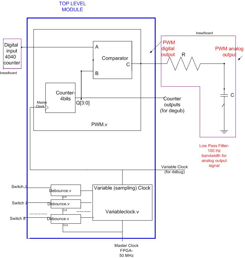
Follow the link Top-Level Module to see the block diagram that illustrates the complete system.
|
|
Gain confidence writing synthesizable multi-module systems. |
|
|
Implement the DAC from lab 3 on the FPGA |
|
|
View the effect that changing the sampling frequency will have on the Digital to Analog Converter analog output |
|
|
Learn how to use the breadboard attached to the Nexys Digilent board. |
|
|
Resistors, capacitors |
|
|
74HC4040 12-stage binary counter |
|
|
Digilent Nexys board based on Xilinx Spartan 3XC2S400 FPGA chip (Can be checked out from the instrument room. You can keep it for the entire quarter; to be returned end of quarter). |
|
|
Digilent FX2-BreadBoard (can be checked out from the instrument room) for this lab only. |
|
|
Xilinx ISE FPGA implementation tools |
|
|
Cadence NC-Simulator (prelab) |
Question1: How many bits does your counter need to divide the 50MHz clock down to 1.5kHz?
Question 2: It is possible or not to achieve a 50MHz clock using the frequency divider provided in class (see PP presentation-clock divider)? What is the maximum frequency that you can achieve?
Question 3: How can you achieve the frequency range mentioned above when you have only 8 input switches?
(Hint: not all inputs to the counter need to come from the switches. Some of
them can be tied to a logic level; which ones, in order to achieve a
high range of frequencies?)
Use slowclock.v and
slowclockTB.v for simulation. Change the value of parameter maxcount!!!
3.Create a Top-Level Module that instantiates the Variable Sampling Frequency Clock Module, the PWM module and the debouncing circuit(s) debounce.v and connect them appropriately.
(A debounceTB.v file is provided in case you want to look at the testbench file and simulation).
4. Create a testbench to verify your Top Level Module design (you may want to verify
using the smaller counter to save simulation time). Be sure to set up your testbench so that the inputs bounce to verify that the debouncing circuits will
correctly eliminate this undesired behavior. Include your *.v file, your testbench file
*_TB.v, and annotated waveforms explaining your simulation results.
5. Study carefully the Design Flow document, valid for Xilinx Webpack ISE 9.2, working under Windows.
6. See http://ece-1.rose-hulman.edu/cadhelp/ to find more information about the software tools used in this lab and the design and the implementation steps.
Link to NEXYS board reference manual
Link to FX2-BreadBoard reference manual
LINK to UCF file for the Digilent Nexys board -
Link to UCF file for FX-2 Bread-Board
A photocopy of your prelab pages is due at the beginning of the class the day before lab.|
|
Clean up your work area |
|
|
Remember to submit your lab notebook for grading at the beginning of next week's lab |
|
|
The lab report should include: |
-The latest version of your Verilog code,
-Prints of the oscilloscope's screen, showing the the PWM Analog output signal, at 3 (three) different sampling frequencies (Low, Medium, High) settings of the equipment that you are using for this lab. State the values of the three frequencies and the corresponding values of the switches.
-"Documentation file" such as the UCF file, Map Report
-Conclusions and/or any special notes regarding this lab ( like problems that you had, how you solved them, debugging issues etc..)