|


| |
 CMOS
Dynamic Behavior CMOS
Dynamic Behavior

Introduction
Objectives
 | Measure gate propagation delay using direct and indirect measurement
methods |
| Measure gate output rise and fall times |
| Investigate relationship between gate switching and supply current spikes |
| Study the effect of decoupling capacitors as a method of reducing supply
noise |
Parts List
| SN74HC04N hex inverter |
| 100 pF capacitor |
| 1000 pF capacitor |
| 0.1 uF capacitor |
| 10-ohm resistor |
Equipment
| Agilent 54622D MSO |
| Agilent 33120A Function/Arb Generator |
| Fixed 5V power supply |
| Breadboard |
Prelab
- Obtain a data sheet for the SN74HC04N hex inverter. Study the “Parameter
Measurement Information” section to determine how to measure rise and fall
times and propagation delay.
- Consider the ring oscillator circuit below:
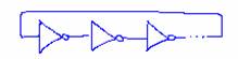
A ring oscillator is a cascade of an odd number of inverters with the final
invert output fed back to the input of the first inverter. The circuit is
self-oscillating, and has no input from another circuit.
Draw the timing diagram for the ring oscillator circuit using N = 5
inverters; the diagram will show all five inverter output waveforms. Assume a
constant finite propagation delay tP for the inverters.
[Hint: Assume that the first inverter has just produced an output transition
from low to high, and hence an input transition to the next inverter of
low to high, then follow the resulting behavior around the loop].
- Derive an equation that describes the oscillation frequency of the ring
oscillator in terms of tP and the number of inverters N.
Explain how this equation could be used to measure propagation delay.
- The supply current IDD is defined as positive when it
enters the VDD pin of a device. Develop a method using an
oscilloscope and a 10-ohm resistor that would allow you to display the dynamic
supply current waveform iDD. Explain your technique and draw
a circuit diagram. [Hint: Remember that the oscilloscopes in our lab must
have their scope probe ground clips attached to ground!]
- Make a photocopy of your prelab pages, and bring to class the day before
lab.
Rise and Fall Time Measurement
- Set up the function generator to produce a 0 to 5V squarewave at 1 MHz.
Apply this signal to a single inverter (the remaining inverter inputs should
be tied low). Monitor both the inverter input and output with the
oscilloscope.
- Adjust the oscilloscope output waveform display to maximize use of the
screen in the vicinity of a rising edge on the inverter output.
- The MSO can measure rise and fall time directly using “Measure -> Quick
Meas” followed by “Softkey -> more” and “Softkey -> Rise Time” (or “Fall
Time”). Note the positions of marker lines, and verify that you understand how
this relates to your Prelab Step 1. Record the rise time tr
and fall time tf of the inverter output and compare to the
published specifications – the data sheet may use the symbol “tt”
to denote transition time when tr and tf
are the same. [Hint: Recall that “compare” is lab handout code for “calculate
percentage error and discuss your findings.”]
- Enter your value for tr under “Topic 1” and tf
under “Topic 2” at
http://www.rose-hulman.edu/~doering/homepage/single-line_comment.htm.
- Repeat Step 3 with a 100 pF capacitive load on the inverter output
(connect between output terminal and ground), and then with a 1000 pF
capacitive load. Discuss the impact of capacitive loading on rise and fall
time.
Propagation Time Measurement
Using the same setup as the previous section, measure the LOW-to-HIGH
propagation delay and the HIGH-to-LOW propagation delay. Compare your results to
the data sheet specifications.
Indirect Measurement of Propagation Delay
- Construct a ring oscillator using N = 5 inverters. Use inverters 1
to 5 of the 74HC04 hex inverter for the ring oscillator. Use the remaining
inverter as a buffer between the ring oscillator and the
instrumentation (frequency counter on the oscilloscope). That is, select one
of the inverter outputs from the ring oscillator, and apply this to the input
of the sixth inverter. Measure the output of the sixth inverter.
- Measure the oscillation frequency of the sixth inverter’s output using the
“quick measurement” feature of the oscilloscope: press “Measure -> Quick Meas”
followed by “Softkey -> Frequency”. You may find it necessary to power cycle
the 74HC04 device a few times to “kick start” the oscillations.
- Enter your frequency measurement from Step 2 under “Topic 3” at
http://www.rose-hulman.edu/~doering/homepage/single-line_comment.htm.
- Once you have a stable reading of frequency, try probing inside the ring
with your other oscilloscope probe. Note any differences in waveform quality,
and note the degree to which the oscilloscope probe alters the measured
frequency. What is the effective capacitance of the probe? (Hint: look at the
probe connection to the oscilloscope).
- Use the equation you derived in the prelab to estimate the propagation
delay tP for a single inverter, and compare to the published
specification and as well as your direct measurement results.
- Study the dependency of propagation delay upon temperature. Try heating
(fingertip) and cooling (ice inside a plastic bag) the package. Determine the
percentage variation in propagation delay for these cases.
- Use the digital probe pod and digital waveform display to create a
measured timing diagram of all five inverter outputs. Compare to your prelab
prediction.
Dynamic Supply Current
- Set up your equipment to display the dynamic supply current iDD.
Seek help from your instructor if you are in doubt about your method!
- Drive one inverter with your 1 MHz squarewave signal (the other
inverters should be tied low). Record the waveform in your lab book and
measure the numerical value of the peak current from your waveform.
- Next, drive two inverters with the same squarewave input signal
(the two inverter inputs would be tied together at this point). Record the
waveform and measure the peak current.
- Repeat the process by driving three inverters, then four, and so forth,
each time recording the waveform and measuring the peak current.
- Plot peak current as a function of the number of simultaneously switched
inverters. Discuss any trends in your data, and propose an explanation for the
trend.
- Now that all six inverters are switching simultaneously, remove the
10-ohm resistor, then look at the dynamic supply voltage vDD
at pin 14. Record the waveform and measure the peak deviation from the
nominal value VDD.
- Connect a 0.1 uF capacitor (called a decoupling capacitor or
bypass capacitor in this application) directly from the VDD
to ground. Make sure that the capacitor is physically close to the package;
you may even want to cut the leads a bit in order to minimize lead length.
- Repeat Step 6. How much did the decoupling capacitor “clean up” the supply
voltage? (Do a percentage change calculation).
- Enter your result from Step 8 under “Topic 4” at
http://www.rose-hulman.edu/~doering/homepage/single-line_comment.htm.
All Done!
| Clean up your work area |
| Remember to submit your lab notebook for grading at the beginning of next
week's lab |
|
