
This week you will design a sequential circuit to be implemented in the GAL chip. The specific sequential circuit that you will implement is a low-cost digital-to-analog converter based on Pulse-Width Modulation technique (PWM).
|
|
Learn the principles of a common type of digital-to-analog converter (D/A or DAC). |
|
|
Design, implement, and test a sequential logic circuit using a GAL PLD. |
|
|
Characterize the performance of your converter. |
|
|
GAL22V10 PLD |
|
|
555 timer (NE555N currently in stock) |
|
|
Resistors, capacitors |
|
|
74HC4040 12-stage binary counter |
|
|
Agilent MSO 7012B mixed-signal oscilloscope (MSO) |
|
|
Digital probes for MSO |
|
|
Agilent 33120A function/arbitrary waveform generator |
|
|
Fixed 5-volt power supply |
|
|
Breadboard |
|
|
USB Thumb Drive |
|
|
Cadence NC-Simulator |
|
|
Lattice ispLEVER: (on lab machines) |
Pulse Width Modulation modules produce digital waveforms that can be used as low-cost digital-to-analog converters with only a few external components. To convert the PWM signal to an analog voltage, a low-pass filter is used.
PWM (Pulse Width Modulation) modules produce digital waveforms, with a variable duty cycle, based on the input signal. In a typical PWM signal, the base frequency (period) is fixed, but the pulse width is variable. The duty cycle varies (from 0% to 100%), proportional with the value of the input signal. (Example: The input pattern 0000 causes the average value of the PWM waveform to be zero, the pattern 0001 causes the average value to be proportional to 1/16, 0010 causes an output average value of 2/16, and so on).
By filtering these pulses , we obtain analog signal proportional with the PWM -module input signal. The LPF will pass the d.c. or average value of the PWM waveforms. PWM modules can be implemented in different ways. One way is explained on the next paragraph-prelab.
Applications of PWM based DACs: stepping motors and motion control, microprocessor-controlled data acquisition systems, generating sounds and complex waveforms, generating variable voltages in a power supply, etc.
In addition to data sheets, IC manufacturers also produce application notes to provide you with ideas to use their products in your own design. Review Microchip Technology’s Application Note AN538, Using PWM to Generate Analog Output, to learn more about the background theory of pulse-width modulation (PWM) as a method of digital-to-analog conversion.
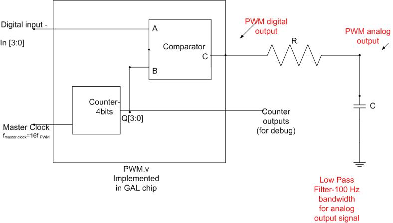
Follow the link PWM DAC system to see the block diagram that illustrates the complete system. The digital part of your system is implemented in the GAL PLD. The four-bit digital input is compared to the current value of the 4-bit free-running counter to determine when the PWM output should be high or low. The PWM output waveform is high until the counter's output becomes equal or greater than the digital input, then it goes low until the counter wraps back to zero and the PWM cycle repeats. The RC analog low-pass filter extracts the average value of the PWM signal to create the final analog output of the converter.
-40dB=-10log[1+(2πfPWM RC)2]
to calculate the value of fPWM
PWM frequency is minimum possible
(permitted by other specifications).
3. Find the Master Clock
Frequency of your system, knowing that PWM waveform Period is 16*Tmaster
clock . (Example: if the Master
clock is 16 KHz, and the digital input is 4 (0100), then the PWM waveform would
be high for 4+1/16 ms and then low for 11/16 ms, so fPMW=1/1ms=1kHz)
4. Write synthesizable Verilog code to implement the digital portion of the PWM DAC
.
The counter must be implemented using four output pins of the GAL, while the
PWM output is a fifth output. The counter output should be observed during
verification in simulation and in hardware.
5. Simulate and verify your design using a testbench. Attach a hardcopy of your Verilog file, your Testbench file, and your waveforms to a lab book page.
Be sure to explain how your waveforms prove that your PWM circuit works.
NOTE: Do not proceed to hardware implementation until your simulation is
100% correct!
A photocopy of your prelab pages is due at the beginning of the class, a day before the lab.
3. Program the GAL chip. Follow the tutorial -Design Flow-Programming GAL ICs using Lattice ispLever
3. Adjust the MSO to display the analog output voltage as the digital input
number varies from zero to fifteen. Try to make the waveform fill the display
so as to get the most amplitude and time resolution. This waveform should look like a stairstep
ramp.
Evaluate the performance of your circuit as a digital-to-analog converter
based on your measurement from Step 3. To what degree is the
output linear?
Clean up your work area
|
|
Remember to submit your lab notebook for grading at the beginning of next week's lab. The lab report should include: |
-Prints of the oscilloscope's screen, showing the digital input signal and the analog output signal and the digital outputs of the PLD (PWM digital signal and the counter's outputs),
-Settings of the equipment that you are using for this lab,
-The 555 astable circuit schematics and calculations,
-"Documentation file" such as the Jedec file and the Chip Report,
-Conclusions and/or any special notes regarding this lab ( like problems that you had, how you solved them, debugging issues etc..)