
|
|
Measure CMOS gates output rise and fall times |
|
|
Measure CMOS gates propagation delay |
|
|
Investigate relationship between gate switching and supply current spikes |
|
|
Study the effect of decoupling capacitors as a method of reducing supply noise |
|
|
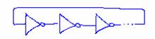
SN74HC04N hex inverter |
|
|
100 pF capacitor |
|
|
1000 pF capacitor |
|
|
0.1 uF capacitor |
|
|
10-ohm resistor |
|
|
Agilent 54622D MSO |
|
|
Agilent 33120A Function/Arb Generator |
|
|
Fixed 5V power supply |
|
|
Breadboard |
Lab Procedures
|
|
Clean up your work area |
|
|
Remember to submit your lab notebook for grading at the end of the lab or the next day. Include prints of the scope for all the steps. Include prints of the oscilloscope with all your measurements, results, conclusions, etc. It is the last ECE 333 lab. |