


PWM-Based Digital-to-Analog Converter
![]()
Introduction
Now you have some experience designing a combinational circuit to be implemented by a programmable logic device, the GAL. This week you will design a sequential circuit to be implemented by the GAL. The specific circuit you will make is a low-cost digital-to-analog converter based on pulse-width modulation (PWM).
Objectives
| Learn the principles of a common type of digital-to-analog converter (D/A or DAC) | |
| Design, implement, and test a sequential logic circuit using a GAL PLD | |
| Characterize the performance of your converter |
Parts List
| GAL22V10 PLD | |
| 555 timer (NE555N currently in stock) | |
| Resistors, capacitors | |
| 74HC4040 12-stage binary counter |
Equipment
| Agilent 54622D mixed-signal oscilloscope (MSO) | |
| Digital probes for MSO | |
| Agilent 33120A function/arbitrary waveform generator | |
| Fixed 5-volt power supply | |
| Breadboard | |
| Floppy Disk |
Software
| Cadence NC-Simulator: Verilog behavioral simulator (download from Tibia) | |
| Lattice ispLEVER: used to convert the design files (on lab machines) |
![]()
Prelab
- In addition to data sheets, IC manufacturers also produce application
notes (“app notes”) to provide you with ideas to use their products in
your own design. Review Microchip Technology’s Application Note AN538,
Using PWM to Generate Analog Output,
to learn more about the background theory of pulse-width modulation
(PWM) as a method of digital-to-analog conversion.
- The diagram below illustrates the complete PWM DAC system:
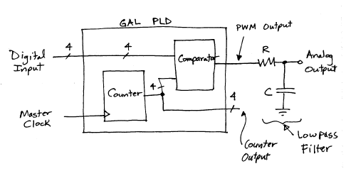
A GAL PLD implements the digital portion of the system. A four-bit digital input is compared to the current "timeslice" indicated by the free-running four-bit counter to determine when the PWM output should be high or low. The RC analog lowpass filter extracts the average value of the PWM signal to create the final analog output of the converter.
- Choose the specific values
of R and C to satisfy the following specifications:
(a) First-order RC filter
(b) 100 Hz bandwidth for analog output signal
(c) At least 40 dB attenuation of fundamental PWM frequency component
(d) PWM frequency is minimum possible permitted by other specifications
The design of your lowpass filter is closely related to the PWM frequency. State the PWM frequency that you will use. State the master clock frequency that you will use.
- Implement the digital portion of the PWM DAC using the Verilog language. The input
pattern 0000 causes the average value of the PWM waveform to be zero, the
pattern 0001 causes the average value to be proportional to 1/16, 0010 causes
an output average value of 2/16, and so on.
The counter must be implemented using four output pins of the GAL, while the PWM output is a fifth output. The counter output should be observed during verification in simulation and in hardware.
- Simulate and verify your design using a testbench circuit. Attach a hardcopy of your
verilog file, your testbench file, and your waveforms to a lab book page.
Be sure to explain how your waveforms prove that your circuit works.
NOTE: Do not proceed to hardware implementation until your simulation is 100% correct!
- A photocopy of your prelab pages is due at the beginning of lab.
Lab
- Build your PWM DAC circuit. Set up the 74HC4040 counter circuit to generate a four-bit input
to your DAC. Use the Agilent 33120A function/arbitrary waveform generator to
generate the squarewave clock signal needed by your counter circuit. The clock
frequency should be selected to fit within the bandwidth of your PWM
converter.
Use a 555-based circuit to create your PWM master clock. Here are some resources: schematic and design equations and data sheet.
- Make hardcopy of the MSO display of the analog output and all digital
outputs of the PLD during one PWM period. Clearly label the traces.
- Adjust the MSO to display the analog output voltage as the digital input
number varies from zero to fifteen. Try to make the waveform fill the display
so as to get the most amplitude and time resolution. This waveform should look like a stairstep
ramp.
- Evaluate the performance of your circuit as a digital-to-analog converter
based on your measurement from Step 3. Do the noise characteristics of the
analog output depend on the specific digital input? To what degree is the
output linear?
- Demonstrate your finished circuit to the instructor.
All done!
| Clean up your work area | |
| Remember to submit your lab notebook for grading at the beginning of next week's lab |